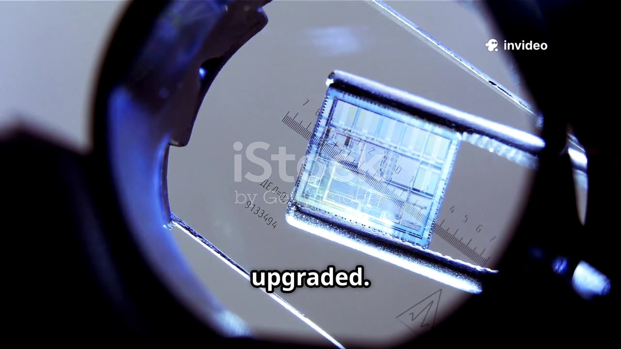
A Common Logic Chip (Conventional) Versus A Chicago Pixel's Common Logic Chip!
Gregory Tarczynski's US Patent 8987873 introduces a "Super Integrated Circuit Chip Semiconductor Device" (CP555) with several key material innovations designed to improve performance over a common logic chip. The patent focuses on a specific combination of materials for the packaging, bonding wires, and substrate to achieve superior thermal, electrical, and radiation resistance properties.
Contrasting Materials and Performance
Element
Common Logic Chip (Conventional)
US Patent 8987873 (CP555)
Package
Typically plastic or ceramic, often made of epoxy-molded compounds, or alumina (Al2O3). These materials have specific operating temperature limits and thermal properties.
Ceramic outer casing of Boron Carbide (B4C). This non-conducting ceramic material is a key feature, providing superior heat resistance and electromagnetic shielding.
Bonding Wire
Usually made of gold (Au), copper (Cu), or aluminum (Al). The choice depends on factors like cost and application. For example, gold is often used for its reliability but is expensive. Copper is a cost-effective alternative.
A custom-formulated Cu-Au-Ag alloy. The patent specifies a range of 5-20% Ag and 5-20% Au by weight in Cu. This alloy is designed to suppress the formation of intermetallic compounds and Kirkendall voids, which degrade bond strength at high temperatures.
Wafer Substrate
Commonly made of Silicon (Si). Silicon is the most widely used semiconductor material, with a well-established manufacturing process.
Heterodiamond substrate layers. This material is used to minimize electro-migration and improve thermal performance. The patent refers to this material in combination with dielectric components.
Dielectric
Often uses silicon dioxide (SiO2) or other low-k dielectric materials for insulation.
The patent specifies the use of Heterodiamond substrates and dielectric components that work together with the Boron Carbide casing to minimize electro-migration.
Export to Sheets
Performance and Reliability Data
Temperature Limits and Thermal Properties
Conventional Chips: The operational temperature for most commercial-grade silicon logic chips is typically 0°C to 70°C, while industrial and military-grade chips can operate from -40°C to 85°C and -55°C to 125°C, respectively. The upper limit is often determined by the packaging materials and bonding wire degradation, with standard gold-to-copper wire bonds degrading at temperatures between 200°C and 325°C due to voiding.
CP555 (US Patent 8987873): The use of a Boron Carbide (B4C) casing and a specialized Cu-Au-Ag alloy bonding wire significantly improves thermal stability. The patent highlights the alloy's ability to maintain tensile strength at high temperatures and suppress degradation mechanisms, suggesting a much higher operational temperature range than conventional chips. This makes it suitable for high-power applications and extreme environments where conventional chips would fail.
Band Gap Width
Conventional Silicon (Si): Silicon, the standard material for a common logic chip's die, has an energy band gap of approximately 1.12 eV. This value is a fundamental property of the material and dictates its electrical behavior, including its temperature-dependent performance.
CP555 (US Patent 8987873): While the patent doesn't explicitly state the band gap of the Heterodiamond substrate, it's known that diamond-like materials, such as diamond itself, have a very wide band gap (around 5.5 eV). Heterodiamond, a composite material containing Boron, Carbon, and Nitrogen, would also likely have a significantly wider band gap than silicon. A wider band gap allows for operation at higher temperatures and voltages before the material's insulating properties break down.
Radiation Hardening
Conventional Chips: Standard silicon chips are susceptible to damage from radiation, which can cause soft errors (temporary malfunctions) or permanent damage. Specialized radiation-hardened chips exist but often come at a higher cost and are based on specific design techniques rather than material changes alone.
CP555 (US Patent 8987873): The patent explicitly claims that the combination of the Boron Carbide (B4C) outer package casing and Heterodiamond substrates and dielectric components provides "superior radiation hardness." This is a key advantage, making the CP555 device ideal for aerospace, military, and nuclear applications where radiation exposure is a major concern.
Dielectric Constants
Conventional Dielectrics: Silicon (Si) has a dielectric constant of approximately 11.7. Common dielectric materials like silicon dioxide (SiO2) have a dielectric constant around 3.9. These values are critical for the design of capacitors and transistors within the chip.
CP555 (US Patent 8987873): The patent does not specify a dielectric constant for the materials used. However, the use of Heterodiamond and other specialized dielectric components is meant to reduce electro-migration, which is a process of atom movement in a conductor due to electron flow. This implies that the materials are engineered for improved insulation and reliability under high current densities, which is an important design consideration for high-performance chips.
_____________________________________________________________________________________________________________________________________________________________________US Patent 8987873: Super Integrated Circuit Chip Semiconductor Device (CP555)
Rewritten for clarity, impact, and educational value Gregory Tarczynski's US Patent 8987873 unveils the "Super Integrated Circuit Chip Semiconductor Device" (CP555), a groundbreaking semiconductor design that leverages advanced materials to deliver superior thermal, electrical, and radiation-resistant performance compared to conventional logic chips. By innovating in the packaging, bonding wires, substrate, and dielectric components, the CP555 sets a new standard for high-performance applications in extreme environments, such as aerospace, military, and nuclear systems.
Material Innovations: CP555 vs. Conventional Logic ChipsThe CP555 introduces a novel combination of materials to enhance reliability, thermal stability, and radiation resistance. Below is a detailed comparison of its key components against those of standard logic chips:
Component
Conventional Logic Chip
CP555 (US Patent 8987873)
Package
Plastic or ceramic (e.g., epoxy-molded compounds or alumina, Al₂O₃). Limited by moderate thermal resistance and operating temperature ranges.
Boron Carbide (B₄C) ceramic casing. Non-conductive, with exceptional heat resistance and electromagnetic shielding for extreme environments.
Bonding Wire
Gold (Au), copper (Cu), or aluminum (Al). Gold is reliable but costly; copper is cost-effective but prone to degradation at high temperatures.
Custom Cu-Au-Ag alloy (5–20% Ag, 5–20% Au by weight in Cu). Reduces intermetallic compound formation and Kirkendall voids, enhancing bond strength at high temperatures.
Wafer Substrate
Silicon (Si). Industry-standard with well-established manufacturing but limited by electro-migration and thermal constraints.
Heterodiamond substrate layers. Minimizes electro-migration and boosts thermal performance for high-power applications.
Dielectric
Silicon dioxide (SiO₂) or low-k dielectrics (e.g., dielectric constant ~3.9). Provides insulation but susceptible to electro-migration under high current.
Heterodiamond-based dielectrics paired with B₄C casing. Engineered to reduce electro-migration and enhance insulation under high current densities.
Performance and Reliability: Key Advantages of CP5551. Enhanced Thermal Stability
Conventional Chips: Most commercial silicon logic chips operate between 0°C and 70°C, with industrial-grade chips extending to -40°C to 85°C and military-grade to -55°C to 125°C. Bonding wire degradation (e.g., gold-to-copper bonds) occurs at 200°C–325°C due to voiding, limiting high-temperature applications.
CP555 Advantage: The Boron Carbide (B₄C) casing and Cu-Au-Ag alloy bonding wire significantly improve thermal stability. The alloy maintains tensile strength at elevated temperatures, suppressing degradation mechanisms like Kirkendall voids and intermetallic compound formation. This enables reliable operation in extreme heat, ideal for high-power and harsh-environment applications.
2. Wide Band Gap for Superior Electrical Performance
Conventional Chips: Silicon substrates have a band gap of ~1.12 eV, which limits their performance at high temperatures and voltages due to increased electron excitation.
CP555 Advantage: The Heterodiamond substrate, a composite of Boron, Carbon, and Nitrogen, likely possesses a band gap closer to diamond’s (~5.5 eV). A wider band gap enhances electrical insulation, enabling the CP555 to operate at higher voltages and temperatures without breakdown, making it suitable for demanding applications.
3. Superior Radiation Hardness
Conventional Chips: Standard silicon chips are vulnerable to radiation-induced soft errors (temporary malfunctions) or permanent damage. Radiation-hardened chips exist but rely on costly design techniques.
CP555 Advantage: The combination of Boron Carbide casing and Heterodiamond substrates provides exceptional radiation hardness, protecting the chip from high-energy particles. This makes the CP555 ideal for aerospace, military, and nuclear applications where radiation exposure is a critical concern.
4. Optimized Dielectric Properties
Conventional Chips: Silicon has a dielectric constant of ~11.7, and silicon dioxide (SiO₂) ~3.9. These materials are prone to electro-migration, where atoms move due to electron flow, degrading performance under high current.
CP555 Advantage: The Heterodiamond-based dielectric, paired with the B₄C casing, minimizes electro-migration, enhancing insulation and reliability under high current densities. While the exact dielectric constant is not specified, the materials are engineered for superior performance in high-performance chips.
Applications and ImpactThe CP555’s innovative material choices—Boron Carbide casing, Cu-Au-Ag alloy bonding wires, and Heterodiamond substrates—position it as a game-changer for industries requiring robust, high-performance semiconductors. Its ability to withstand extreme temperatures, high voltages, and radiation makes it uniquely suited for:
Aerospace: Reliable operation in satellites and spacecraft exposed to cosmic radiation.
Military: Durable performance in rugged, high-temperature environments.
Nuclear: Resistance to radiation in power plants and research facilities.
High-Power Electronics: Enhanced thermal and electrical performance for cutting-edge computing and power systems.
Educational InsightsThe CP555 exemplifies how material science advancements can push semiconductor technology beyond the limitations of silicon-based designs. Key concepts highlighted by the patent include:
Band Gap: A wider band gap (e.g., Heterodiamond vs. Silicon) improves a material’s ability to operate at higher temperatures and voltages.
Electro-migration: The movement of atoms in a conductor due to electron flow, which can degrade chip performance. The CP555’s materials are designed to mitigate this issue.
Radiation Hardness: Critical for applications in radiation-heavy environments, achieved through material innovations rather than solely design techniques.
Thermal Management: Advanced packaging and bonding materials, like B₄C and Cu-Au-Ag alloys, enable chips to handle extreme heat without compromising reliability.
By integrating these principles, the CP555 not only enhances performance but also sets a foundation for future semiconductor innovations in extreme-environment applications.
For further details on the patent, refer to US Patent 8987873.
Explain Heterodiamond properties
Heterodiamond, as referenced in US Patent 8987873, is a composite material primarily composed of boron, carbon, and nitrogen, often referred to as boron-carbon-nitrogen (BCN) or related compounds like boron nitride (BN) or carbon-doped boron nitride. While the patent does not provide an exhaustive breakdown of its exact composition, Heterodiamond is designed to enhance the performance of the CP555 semiconductor device through its unique electrical, thermal, and mechanical properties. Below is an explanation of its key properties, grounded in the context of the patent and general knowledge of similar materials.Key Properties of Heterodiamond
1. Wide Band Gap
Description: Heterodiamond likely has a wide energy band gap, potentially in the range of 4–5.5 eV, similar to diamond (5.5 eV) or cubic boron nitride (c-BN, ~6 eV), compared to silicon’s 1.12 eV.
Significance: A wide band gap allows Heterodiamond to function as an excellent insulator, resisting electron excitation at high temperatures and voltages. This enables the CP555 to operate reliably in extreme conditions, such as high-power electronics or aerospace applications.
Application in CP555: The wide band gap enhances the substrate’s ability to handle high electric fields, reducing the risk of electrical breakdown in demanding environments.
2. High Thermal Conductivity
Description: Heterodiamond inherits high thermal conductivity from its diamond-like structure, potentially exceeding 2000 W/m·K (comparable to diamond) and far surpassing silicon (~150 W/m·K).
Significance: This property allows efficient heat dissipation, critical for maintaining performance in high-power or high-temperature settings where conventional silicon substrates struggle.
Application in CP555: The patent highlights Heterodiamond’s role in improving thermal performance, enabling the CP555 to operate at elevated temperatures without degradation.
3. Low Electro-Migration
Description: Electro-migration, the movement of atoms in a conductor due to electron flow, is minimized in Heterodiamond due to its robust atomic structure and dielectric properties.
Significance: Reduced electro-migration enhances the longevity and reliability of the CP555 under high current densities, preventing performance degradation in transistors and interconnects.
Application in CP555: The patent specifies that Heterodiamond substrates and dielectric components work with the boron carbide (B₄C) casing to suppress electro-migration, ensuring stable operation in high-performance chips.
4. High Radiation Hardness
Description: Heterodiamond’s strong covalent bonding and wide band gap make it resistant to radiation-induced damage, such as soft errors or lattice defects caused by high-energy particles.
Significance: This property protects the chip from radiation in environments like space, nuclear facilities, or military applications, where conventional silicon chips are vulnerable.
Application in CP555: The patent emphasizes "superior radiation hardness" achieved through the combination of Heterodiamond and boron carbide, making the CP555 ideal for extreme environments.
5. Mechanical Strength and Hardness
Description: Heterodiamond shares the extreme hardness of diamond and cubic boron nitride, with a Vickers hardness potentially approaching 70–100 GPa (diamond is ~100 GPa).
Significance: Its mechanical durability ensures structural integrity under physical stress or thermal cycling, preventing cracks or failures in the substrate or dielectric layers.
Application in CP555: This property supports the chip’s reliability in rugged applications, complementing the boron carbide casing’s durability.
6. Dielectric Properties
Description: Heterodiamond likely has a low dielectric constant (potentially 5–7, compared to silicon’s 11.7 or SiO₂’s 3.9) and high dielectric strength, making it an effective insulator for high-frequency and high-voltage applications.
Significance: A low dielectric constant reduces parasitic capacitance, improving signal integrity and speed in high-performance circuits. High dielectric strength prevents breakdown under intense electric fields.
Application in CP555: The patent notes that Heterodiamond-based dielectrics, paired with the B₄C casing, enhance insulation and reduce electro-migration, optimizing the chip for high current densities.
7. Chemical Stability
Description: Heterodiamond’s diamond-like structure provides excellent resistance to chemical degradation, corrosion, and oxidation, even at high temperatures.
Significance: This ensures long-term reliability in harsh environments, such as those with high humidity, corrosive gases, or extreme thermal cycling.
Application in CP555: Chemical stability complements the thermal and radiation resistance, making the CP555 suitable for prolonged use in extreme conditions.
Comparison to Conventional Materials
Silicon (Si): Silicon, with a band gap of 1.12 eV and thermal conductivity of ~150 W/m·K, is less effective at high temperatures and voltages and more susceptible to radiation damage.
Silicon Dioxide (SiO₂): Commonly used as a dielectric, SiO₂ has a dielectric constant of ~3.9 but is prone to electro-migration and has lower thermal conductivity.
Heterodiamond Advantage: Its wider band gap, higher thermal conductivity, and superior radiation hardness make it a superior choice for the CP555’s substrate and dielectric layers, enabling performance in conditions where silicon-based chips fail.
Educational Insights
Band Gap: The energy difference between a material’s valence and conduction bands. A wider band gap (like Heterodiamond’s) allows operation at higher temperatures and voltages without electron leakage.
Thermal Conductivity: Measures a material’s ability to conduct heat. Heterodiamond’s high thermal conductivity prevents overheating, a critical factor in high-power chips.
Electro-Migration: The displacement of atoms due to electron flow, which can degrade conductors. Heterodiamond’s structure minimizes this, enhancing chip longevity.
Radiation Hardness: Resistance to radiation-induced defects, crucial for applications in space or nuclear environments.
Applications in CP555The Heterodiamond substrate and dielectric components in the CP555 enable:
Operation in extreme temperatures (potentially >200°C).
Resistance to radiation in aerospace, military, and nuclear settings.
Enhanced reliability under high current and voltage, ideal for high-performance computing and power electronics.
Improved signal integrity and speed due to low dielectric constant and high dielectric strength.
By leveraging Heterodiamond’s exceptional properties, the CP555 achieves unparalleled performance, making it a transformative solution for next-generation semiconductor applications.
____________________________________________________________________________________________________________________________________________________
US Patent 8987873: Super Integrated Circuit Chip Semiconductor Device (CP555)
Rewritten for clarity, impact, and educational value Gregory Tarczynski's US Patent 8987873 unveils the "Super Integrated Circuit Chip Semiconductor Device" (CP555), a groundbreaking semiconductor design that leverages advanced materials to deliver superior thermal, electrical, and radiation-resistant performance compared to conventional logic chips. By innovating in the packaging, bonding wires, substrate, and dielectric components, the CP555 sets a new standard for high-performance applications in extreme environments, such as aerospace, military, and nuclear systems.
Material Innovations: CP555 vs. Conventional Logic ChipsThe CP555 introduces a novel combination of materials to enhance reliability, thermal stability, and radiation resistance. Below is a detailed comparison of its key components against those of standard logic chips:
Component
Conventional Logic Chip
CP555 (US Patent 8987873)
Package
Plastic or ceramic (e.g., epoxy-molded compounds or alumina, Al₂O₃). Limited by moderate thermal resistance and operating temperature ranges.
Boron Carbide (B₄C) ceramic casing. Non-conductive, with exceptional heat resistance and electromagnetic shielding for extreme environments.
Bonding Wire
Gold (Au), copper (Cu), or aluminum (Al). Gold is reliable but costly; copper is cost-effective but prone to degradation at high temperatures.
Custom Cu-Au-Ag alloy (5–20% Ag, 5–20% Au by weight in Cu). Reduces intermetallic compound formation and Kirkendall voids, enhancing bond strength at high temperatures.
Wafer Substrate
Silicon (Si). Industry-standard with well-established manufacturing but limited by electro-migration and thermal constraints.
Heterodiamond substrate layers. Minimizes electro-migration and boosts thermal performance for high-power applications.
Dielectric
Silicon dioxide (SiO₂) or low-k dielectrics (e.g., dielectric constant ~3.9). Provides insulation but susceptible to electro-migration under high current.
Heterodiamond-based dielectrics paired with B₄C casing. Engineered to reduce electro-migration and enhance insulation under high current densities.
Performance and Reliability: Key Advantages of CP5551. Enhanced Thermal Stability
Conventional Chips: Most commercial silicon logic chips operate between 0°C and 70°C, with industrial-grade chips extending to -40°C to 85°C and military-grade to -55°C to 125°C. Bonding wire degradation (e.g., gold-to-copper bonds) occurs at 200°C–325°C due to voiding, limiting high-temperature applications.
CP555 Advantage: The Boron Carbide (B₄C) casing and Cu-Au-Ag alloy bonding wire significantly improve thermal stability. The alloy maintains tensile strength at elevated temperatures, suppressing degradation mechanisms like Kirkendall voids and intermetallic compound formation. This enables reliable operation in extreme heat, ideal for high-power and harsh-environment applications.
2. Wide Band Gap for Superior Electrical Performance
Conventional Chips: Silicon substrates have a band gap of ~1.12 eV, which limits their performance at high temperatures and voltages due to increased electron excitation.
CP555 Advantage: The Heterodiamond substrate, a composite of Boron, Carbon, and Nitrogen, likely possesses a band gap closer to diamond’s (~5.5 eV). A wider band gap enhances electrical insulation, enabling the CP555 to operate at higher voltages and temperatures without breakdown, making it suitable for demanding applications.
3. Superior Radiation Hardness
Conventional Chips: Standard silicon chips are vulnerable to radiation-induced soft errors (temporary malfunctions) or permanent damage. Radiation-hardened chips exist but rely on costly design techniques.
CP555 Advantage: The combination of Boron Carbide casing and Heterodiamond substrates provides exceptional radiation hardness, protecting the chip from high-energy particles. This makes the CP555 ideal for aerospace, military, and nuclear applications where radiation exposure is a critical concern.
4. Optimized Dielectric Properties
Conventional Chips: Silicon has a dielectric constant of ~11.7, and silicon dioxide (SiO₂) ~3.9. These materials are prone to electro-migration, where atoms move due to electron flow, degrading performance under high current.
CP555 Advantage: The Heterodiamond-based dielectric, paired with the B₄C casing, minimizes electro-migration, enhancing insulation and reliability under high current densities. While the exact dielectric constant is not specified, the materials are engineered for superior performance in high-performance chips.
Applications and ImpactThe CP555’s innovative material choices—Boron Carbide casing, Cu-Au-Ag alloy bonding wires, and Heterodiamond substrates—position it as a game-changer for industries requiring robust, high-performance semiconductors. Its ability to withstand extreme temperatures, high voltages, and radiation makes it uniquely suited for:
Aerospace: Reliable operation in satellites and spacecraft exposed to cosmic radiation.
Military: Durable performance in rugged, high-temperature environments.
Nuclear: Resistance to radiation in power plants and research facilities.
High-Power Electronics: Enhanced thermal and electrical performance for cutting-edge computing and power systems.
Educational InsightsThe CP555 exemplifies how material science advancements can push semiconductor technology beyond the limitations of silicon-based designs. Key concepts highlighted by the patent include:
Band Gap: A wider band gap (e.g., Heterodiamond vs. Silicon) improves a material’s ability to operate at higher temperatures and voltages.
Electro-migration: The movement of atoms in a conductor due to electron flow, which can degrade chip performance. The CP555’s materials are designed to mitigate this issue.
Radiation Hardness: Critical for applications in radiation-heavy environments, achieved through material innovations rather than solely design techniques.
Thermal Management: Advanced packaging and bonding materials, like B₄C and Cu-Au-Ag alloys, enable chips to handle extreme heat without compromising reliability.
By integrating these principles, the CP555 not only enhances performance but also sets a foundation for future semiconductor innovations in extreme-environment applications.
For further details on the patent, refer to US Patent 8987873.
Explain Heterodiamond properties
Heterodiamond, as referenced in US Patent 8987873, is a composite material primarily composed of boron, carbon, and nitrogen, often referred to as boron-carbon-nitrogen (BCN) or related compounds like boron nitride (BN) or carbon-doped boron nitride. While the patent does not provide an exhaustive breakdown of its exact composition, Heterodiamond is designed to enhance the performance of the CP555 semiconductor device through its unique electrical, thermal, and mechanical properties. Below is an explanation of its key properties, grounded in the context of the patent and general knowledge of similar materials.Key Properties of Heterodiamond
1. Wide Band Gap
Description: Heterodiamond likely has a wide energy band gap, potentially in the range of 4–5.5 eV, similar to diamond (5.5 eV) or cubic boron nitride (c-BN, ~6 eV), compared to silicon’s 1.12 eV.
Significance: A wide band gap allows Heterodiamond to function as an excellent insulator, resisting electron excitation at high temperatures and voltages. This enables the CP555 to operate reliably in extreme conditions, such as high-power electronics or aerospace applications.
Application in CP555: The wide band gap enhances the substrate’s ability to handle high electric fields, reducing the risk of electrical breakdown in demanding environments.
2. High Thermal Conductivity
Description: Heterodiamond inherits high thermal conductivity from its diamond-like structure, potentially exceeding 2000 W/m·K (comparable to diamond) and far surpassing silicon (~150 W/m·K).
Significance: This property allows efficient heat dissipation, critical for maintaining performance in high-power or high-temperature settings where conventional silicon substrates struggle.
Application in CP555: The patent highlights Heterodiamond’s role in improving thermal performance, enabling the CP555 to operate at elevated temperatures without degradation.
3. Low Electro-Migration
Description: Electro-migration, the movement of atoms in a conductor due to electron flow, is minimized in Heterodiamond due to its robust atomic structure and dielectric properties.
Significance: Reduced electro-migration enhances the longevity and reliability of the CP555 under high current densities, preventing performance degradation in transistors and interconnects.
Application in CP555: The patent specifies that Heterodiamond substrates and dielectric components work with the boron carbide (B₄C) casing to suppress electro-migration, ensuring stable operation in high-performance chips.
4. High Radiation Hardness
Description: Heterodiamond’s strong covalent bonding and wide band gap make it resistant to radiation-induced damage, such as soft errors or lattice defects caused by high-energy particles.
Significance: This property protects the chip from radiation in environments like space, nuclear facilities, or military applications, where conventional silicon chips are vulnerable.
Application in CP555: The patent emphasizes "superior radiation hardness" achieved through the combination of Heterodiamond and boron carbide, making the CP555 ideal for extreme environments.
5. Mechanical Strength and Hardness
Description: Heterodiamond shares the extreme hardness of diamond and cubic boron nitride, with a Vickers hardness potentially approaching 70–100 GPa (diamond is ~100 GPa).
Significance: Its mechanical durability ensures structural integrity under physical stress or thermal cycling, preventing cracks or failures in the substrate or dielectric layers.
Application in CP555: This property supports the chip’s reliability in rugged applications, complementing the boron carbide casing’s durability.
6. Dielectric Properties
Description: Heterodiamond likely has a low dielectric constant (potentially 5–7, compared to silicon’s 11.7 or SiO₂’s 3.9) and high dielectric strength, making it an effective insulator for high-frequency and high-voltage applications.
Significance: A low dielectric constant reduces parasitic capacitance, improving signal integrity and speed in high-performance circuits. High dielectric strength prevents breakdown under intense electric fields.
Application in CP555: The patent notes that Heterodiamond-based dielectrics, paired with the B₄C casing, enhance insulation and reduce electro-migration, optimizing the chip for high current densities.
7. Chemical Stability
Description: Heterodiamond’s diamond-like structure provides excellent resistance to chemical degradation, corrosion, and oxidation, even at high temperatures.
Significance: This ensures long-term reliability in harsh environments, such as those with high humidity, corrosive gases, or extreme thermal cycling.
Application in CP555: Chemical stability complements the thermal and radiation resistance, making the CP555 suitable for prolonged use in extreme conditions.
Comparison to Conventional Materials
Silicon (Si): Silicon, with a band gap of 1.12 eV and thermal conductivity of ~150 W/m·K, is less effective at high temperatures and voltages and more susceptible to radiation damage.
Silicon Dioxide (SiO₂): Commonly used as a dielectric, SiO₂ has a dielectric constant of ~3.9 but is prone to electro-migration and has lower thermal conductivity.
Heterodiamond Advantage: Its wider band gap, higher thermal conductivity, and superior radiation hardness make it a superior choice for the CP555’s substrate and dielectric layers, enabling performance in conditions where silicon-based chips fail.
Educational Insights
Band Gap: The energy difference between a material’s valence and conduction bands. A wider band gap (like Heterodiamond’s) allows operation at higher temperatures and voltages without electron leakage.
Thermal Conductivity: Measures a material’s ability to conduct heat. Heterodiamond’s high thermal conductivity prevents overheating, a critical factor in high-power chips.
Electro-Migration: The displacement of atoms due to electron flow, which can degrade conductors. Heterodiamond’s structure minimizes this, enhancing chip longevity.
Radiation Hardness: Resistance to radiation-induced defects, crucial for applications in space or nuclear environments.
Applications in CP555The Heterodiamond substrate and dielectric components in the CP555 enable:
Operation in extreme temperatures (potentially >200°C).
Resistance to radiation in aerospace, military, and nuclear settings.
Enhanced reliability under high current and voltage, ideal for high-performance computing and power electronics.
Improved signal integrity and speed due to low dielectric constant and high dielectric strength.
By leveraging Heterodiamond’s exceptional properties, the CP555 achieves unparalleled performance, making it a transformative solution for next-generation semiconductor applications.For further details, refer to US Patent 8987873.
Compare to other substrates
To compare Heterodiamond, as described in US Patent 8987873 for the CP555 semiconductor device, to other commonly used semiconductor substrates, we’ll evaluate it against silicon (Si), silicon carbide (SiC), gallium arsenide (GaAs), and gallium nitride (GaN). These substrates are widely used in logic chips, power electronics, and high-frequency applications. The comparison focuses on key properties relevant to semiconductor performance: band gap, thermal conductivity, electron mobility, dielectric constant, radiation hardness, and mechanical strength. This analysis provides an educational overview of how Heterodiamond stands out for high-performance applications in extreme environments.
Comparison Table: Heterodiamond vs. Other Substrates
Property
Heterodiamond (CP555)
Silicon (Si)
Silicon Carbide (SiC)
Gallium Arsenide (GaAs)
Gallium Nitride (GaN)
Band Gap (eV)
Likely 4–5.5 eV (similar to diamond or cubic boron nitride, c-BN)
1.12 (indirect)
3.26 (4H-SiC, wide, indirect)
1.43 (direct)
3.4 (wide, direct)
Thermal Conductivity (W/m·K)
~2000 (comparable to diamond)
~150
~370–490 (4H-SiC)
~55
~130–200
Electron Mobility (cm²/V·s)
Not specified; likely moderate due to composite nature (~1000, estimated from c-BN)
~1350 (n-type)
~900 (4H-SiC)
~8500 (high, ideal for high-frequency)
~1200–2000
Dielectric Constant
~5–7 (estimated, low for diamond-like materials)
11.7
~9.7 (4H-SiC)
~12.9
~8.9
Radiation Hardness
Superior (due to strong covalent bonding and wide band gap)
Poor (susceptible to soft errors and permanent damage)
Good (wide band gap reduces radiation-induced defects)
Moderate (better than Si but less than SiC or GaN)
Good (wide band gap, suitable for space applications)
Mechanical Strength
Extremely high (~70–100 GPa Vickers hardness, similar to diamond)
Moderate (~7 GPa)
High (~20–30 GPa)
Low (~4–6 GPa, brittle)
High (~15–20 GPa)
Chemical Stability
Excellent (resists corrosion, oxidation, even at high temperatures)
Good (oxidizes at high temperatures)
Excellent (resists harsh chemical environments)
Moderate (susceptible to chemical degradation)
Excellent (highly stable in harsh conditions)
Primary Applications
Extreme environments (aerospace, military, nuclear), high-power, high-temperature devices
General-purpose logic chips, microprocessors, memory
Power electronics, high-temperature, high-voltage devices
High-frequency, optoelectronics (LEDs, lasers)
Power electronics, RF devices, optoelectronics (UV LEDs)
Cost
Likely high (due to complex BCN composite synthesis)
Low (mature, widely available)
Moderate to high (specialized production)
High (complex manufacturing)
High (emerging, specialized processes)
Detailed Comparison
1. Band Gap
Heterodiamond: Likely 4–5.5 eV (based on diamond/c-BN). A wide band gap enables operation at high temperatures and voltages, ideal for extreme environments like aerospace or nuclear applications.
Silicon: 1.12 eV (indirect). Limited to moderate temperatures and voltages due to electron excitation.
Silicon Carbide: 3.26 eV (4H-SiC). Wide band gap supports high-voltage and high-temperature applications, but less than Heterodiamond.
Gallium Arsenide: 1.43 eV (direct). Better for high-frequency and optoelectronic applications but not suited for extreme temperatures.
Gallium Nitride: 3.4 eV (direct). Excellent for high-voltage and high-frequency devices but still below Heterodiamond’s band gap.
Advantage: Heterodiamond’s wider band gap offers superior electrical insulation and thermal stability, making it ideal for the CP555’s extreme-condition applications.
2. Thermal Conductivity
Heterodiamond: ~2000 W/m·K (diamond-like). Exceptional heat dissipation, critical for high-power devices.
Silicon: ~150 W/m·K. Adequate for general-purpose chips but insufficient for high-power or high-temperature settings.
Silicon Carbide: ~370–490 W/m·K. Very good, supporting power electronics in harsh conditions.
Gallium Arsenide: ~55 W/m·K. Poor thermal conductivity limits its use in high-power applications.
Gallium Nitride: ~130–200 W/m·K. Good but significantly lower than Heterodiamond or SiC.
Advantage: Heterodiamond’s unmatched thermal conductivity ensures the CP555 can handle intense heat, preventing performance degradation.
3. Electron Mobility
Heterodiamond: Not specified in the patent; likely moderate (~1000 cm²/V·s, estimated from c-BN). May not prioritize high-frequency performance.
Silicon: ~1350 cm²/V·s. Good for general-purpose electronics but limited by lower band gap.
Silicon Carbide: ~900 cm²/V·s (4H-SiC). Lower mobility but compensated by high voltage tolerance.
Gallium Arsenide: ~8500 cm²/V·s. Excellent for high-frequency applications like RF and optoelectronics.
Gallium Nitride: ~1200–2000 cm²/V·s. Strong for RF and power electronics.
Advantage: GaAs excels in high-frequency applications, but Heterodiamond’s focus is on thermal and radiation resilience rather than speed.
4. Dielectric Constant
Heterodiamond: ~5–7 (estimated). Low dielectric constant reduces parasitic capacitance, improving signal integrity.
Silicon: 11.7. Higher capacitance can slow signal propagation.
Silicon Carbide: ~9.7. Better than silicon but not as low as Heterodiamond.
Gallium Arsenide: ~12.9. High capacitance limits high-frequency performance in some cases.
Gallium Nitride: ~8.9. Good but higher than Heterodiamond.
Advantage: Heterodiamond’s lower dielectric constant enhances performance in high-frequency and high-power circuits, as noted in the CP555’s design.
5. Radiation Hardness
Heterodiamond: Superior due to strong covalent bonding and wide band gap, ideal for aerospace and nuclear applications.
Silicon: Poor; susceptible to soft errors and permanent damage from radiation.
Silicon Carbide: Good; wide band gap reduces radiation sensitivity, used in space applications.
Gallium Arsenide: Moderate; better than silicon but less robust than SiC or GaN.
Gallium Nitride: Good; suitable for radiation-heavy environments like space.
Advantage: Heterodiamond’s exceptional radiation hardness, paired with boron carbide casing, makes the CP555 unmatched for extreme radiation environments.
6. Mechanical Strength
Heterodiamond: ~70–100 GPa (Vickers hardness). Extremely durable, resisting cracks under thermal or mechanical stress.
Silicon: ~7 GPa. Moderate, prone to cracking under stress.
Silicon Carbide: ~20–30 GPa. Strong, suitable for rugged applications.
Gallium Arsenide: ~4–6 GPa. Brittle, limiting physical durability.
Gallium Nitride: ~15–20 GPa. Strong but less than SiC or Heterodiamond.
Advantage: Heterodiamond’s diamond-like hardness ensures structural integrity in the CP555 under harsh conditions.
7. Cost and Manufacturability
Heterodiamond: Likely expensive due to complex synthesis (e.g., chemical vapor deposition of BCN composites).
Silicon: Low cost, mature manufacturing processes.
Silicon Carbide: Moderate to high cost, specialized production.
Gallium Arsenide: High cost, complex fabrication.
Gallium Nitride: High cost, emerging technology.
Advantage: Silicon is the most cost-effective, but Heterodiamond’s premium properties justify its cost for specialized applications.
Educational Insights
Band Gap: Determines a material’s ability to insulate at high temperatures/voltages. Wider band gaps (Heterodiamond, SiC, GaN) excel in extreme conditions.
Thermal Conductivity: Critical for heat dissipation in high-power devices. Heterodiamond’s diamond-like conductivity is a standout.
Electron Mobility: Higher mobility (e.g., GaAs) suits high-frequency applications, while Heterodiamond prioritizes thermal and radiation resilience.
Radiation Hardness: Wide-band-gap materials (Heterodiamond, SiC, GaN) resist radiation damage, crucial for space and nuclear use.
Electro-Migration: Heterodiamond’s low dielectric constant and robust structure minimize atom displacement, enhancing reliability.
Why Heterodiamond for CP555?Heterodiamond’s combination of a wide band gap, exceptional thermal conductivity, low dielectric constant, and superior radiation hardness makes it uniquely suited for the CP555’s target applications:
Extreme Environments: Aerospace, military, and nuclear settings benefit from radiation and thermal resilience.
High-Power Electronics: Efficient heat dissipation and low electro-migration support high current density.
Reliability: Mechanical strength and chemical stability ensure long-term performance under stress.
While silicon remains the go-to for cost-effective, general-purpose chips, and SiC/GaN excel in power and RF applications, Heterodiamond’s diamond-like properties push the boundaries for extreme-condition semiconductors, as envisioned in US Patent 8987873.
-
 1:57:22
The Charlie Kirk Show
2 hours agoTucker Carlson on the Faith of Charlie Kirk | 9.19.2025
113K86 -
 LIVE
LIVE
Dr Disrespect
3 hours ago🔴LIVE - DR DISRESPECT - SUPER ENTERTAINMENT POWER
1,367 watching -
 LIVE
LIVE
Lara Logan
6 hours agoTHE FIGHT FOR A FREE BRITAIN with Katie Hopkins | Episode 36 | Going Rogue with Lara Logan
593 watching -
 16:52
16:52
IsaacButterfield
9 hours ago $0.11 earnedWoke Karens Are Trying to End This Man’s Career
902 -
 4:09:14
The Bubba Army
1 day agoRaja Jackson Arrested! - Bubba the Love Sponge® Show | 9/19/25
13K1 -
 2:04:42
The Culture War with Tim Pool
3 hours agoDemonic Possession, Exorcisms, And The Soul Of America | The Culture War with Tim Pool
140K125 -
 20:00
20:00
Neil McCoy-Ward
2 hours ago🔥 It's Absolute CHAOS In Europe 🇪🇺 Today...
18.2K5 -
 1:07:41
Steven Crowder
4 hours agoSPECIAL: A Behind-the-Scenes Peek at Some of Our Biggest Productions
218K101 -
 59:40
59:40
The Rubin Report
4 hours agoListen to ‘The View’ Crowd Gasp as Whoopi Admits She Agrees w/ Conservatives on This
67.1K33 -
 1:40:02
The Mel K Show
3 hours agoMORNINGS WITH MEL K Preserving the Home of the Brave 9-19-25
46.4K5